

“Science is messy, and the results of research rarely conform fully to plan or expectation. ‘Clean’ narratives are an artefact of inappropriate pressures and the culture they have generated.”
Tell it like it is. Nat Hum Behav 4, 1 (2020)
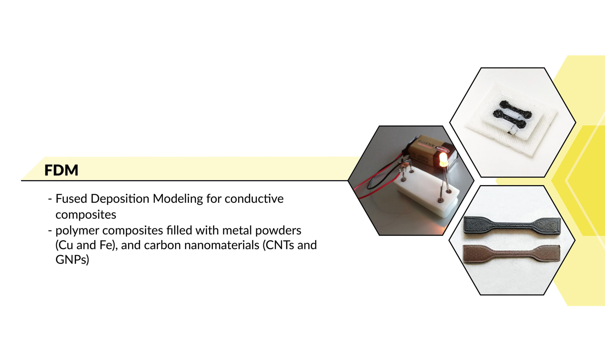
The main objective of this project is to design, fabricate and characterise a group of composite materials with tailored physical properties for additive manufacturing of structural electronics. A vast range of investigations will be conducted on fabrication of polymer composites with metal, carbon, ceramic, semiconductor, and other type of functional phases – including, but not limited to nanomaterials – with emphasis on rheology, dispersion and homogenization, electrical properties (resistivity, dielectric properties, noises), mechanical and environmental factors and other functional properties (optical, magnetic, piezo, thermal, etc.).
Research will be conducted taking into account final application of elaborated materials in Fussed Deposition Modelling, Direct Write, Selective Laser Sintering and PolyJet or Aerosol Jet Printing. Series of demonstrators will be prepared with the use of obtained materials. Series of demonstrators will be prepared, including: electric motor, battery or capacitor, loudspeaker, USB keyboard, 3D electronic circuits, and ultimate demonstrator – a simple, functional robot with microcontroller.
SIGNIFICANCE
Structural electronics is a therm describing electrical and electronic components and circuits that act as construction elements, casings or other type of protective dumb structures (like vehicle bodies), embedded inside the volume of element or conformally placed on the surface. Due to possibility of enhancing products functionality, lowering production cost, or providing possibility for fabrication of consumer tailored devices, structural electronics is an interesting new branch of technology for aerospace and military applications, home appliances, consumer electronics, automotive industry and civil engineering. Realisation format for structural electronics is mostly provided by fitting standard geometry components into spare spaces in machines, tailoring shape of conventional components to fit into spare space, adding conformal coating – a “smart skin” – on the surface of existing elements (sensors, photovoltaics), in-mould shaping of multilayer electronics (home appliance casings or car audio) or finally forming as load bearing elements (bridges, houses, cars). Enhancing functionality by addition of “smart skin” or elastic shaped elements can be realised by using printed and elastic electronics, but the load bearing or construction elements needs more complex solutions, like laminating, in-mold shaping, injection moulding, casting or finally 3D printing. At the present time we should ask the question: which components are most suitable for fabrication and implementation in structural electronics? Simple conductive elements, antennas, interconnects, actuators and photovoltaics can be readily adapted in the volume/surface of the construction elements, moving parts, in narrow spaces or on the curved shapes. Bigger problems is with power elements like supercapacitors, batteries, fuel cells and electric motors. These elements cannot be fabricated as surface coatings (with exception to capacitors and batteries), and usually they will carve large volume of element.
One of the disruptive manufacturing technique, with significant impact on many fields of technology is additive manufacturing called also rapid prototyping, or 3D printing. It allows to fabricate objects directly from digital computer aided design (CAD) files, without moulding or subtractive milling. It allows to design complex geometry parts, permit fast and flexible design changes, and prompt development of mass customisation. Engineers are using 3D printing since more than a decade to make models and prototypes, mainly in the form of visual aids. However, more recently the technology has found greater appeal in final-product manufacturing across diverse fields, from medical implants to the artistic realisations. Furthermore, the technology provides a low-risk entrance to market for innovations.
In parallel to 3D printing we deal with printed electronics, another revolutionary additive technology involving vast experience of printing industry. Printed electronics is not meant to be the opponent of silicon chips and PCB’s, rather a complementary partner in manufacturing processes, especially in the production of low-cost and large-area systems. Many electronic solutions are already produced with printed electronics techniques, including RFID tags, photovoltaic cells, sensors, electroluminescent displays, batteries, capacitors and many others. As an additive technology it allows more efficient utilisation of materials. With decades of development behind printed electronics systems (starting from thick film technology in late 70’s), they are reliable, fast, and inexpensive. Their primary limitation is deposition of functional material only on flat substrates, though flexible circuits are also possible. The resulting electronics becomes a separate component from the structure of the final product.
GOAL
Most of the 3D printers build elements from one type of material, and they are incapable to build objects with electronic, optical, or any kind of functions that require integration of multiple materials. Combining results of additive manufacturing and printed electronics, the concepts for integration of 3D printing and conductive materials for producing functional, monolithic 3D structures with embedded electronics emerged. Structural electronics produced by 3D printing will function much like printed electronics, with the advantage of production of 3D objects with the wires and circuitry embedded in volume of element. This allow designers to create products smaller, lighter, more efficient, and customised. To achieve this goal, low-cost, easy to use functional materials and 3D printing methodologies are required.
The crucial aspect for rapid development of 3D printed structural electronics are functional materials. With the use of FDM, ink-jet, aerosol printing, direct write (paste extrusion) or other techniques, conductive, insulating and functional inks, pastes and composites will form final solution. The most promising group of materials will be conductive thermoplastic filaments and conductive inks and pastes. At this time at least a dozen of companies is working on supplying such technologies to the market, but they objectives are narrow and straightforward – the lowest possible resistivity – what limits practical applications. A carbon-composite inks are developed for 3D printing applications and graphene-based inks with enhanced functionality and improved electrical, mechanical, and biological properties.
The main hypothesis that will be validated during the project is that tailoring properties of composite materials with metallic, carbon, ceramic and semiconducting materials (including nanomaterials) allows for significant enhancement of physical properties (electrical, optical, mechanical, thermal, etc) required for high performance structural electronics, comparing to the state of the art silver pastes and carbon filled composites.
Our goal can be described in several tasks proposed in the project.
1. Determination of critical physical materials properties relative for electronics materials application
2. Modelling of determined physical properties in composite materials with finite elements analysis tools
3. Research and selection of functional phase materials for elaboration of electronic composites
4. Elaboration and fabrication of electronic materials with optimisation of their composition
5. Elaboration and fabrication of 3D printed test structures
6. Detailed studies on physical properties of samples
7. Preparation of electrical, electronic and mechatronic demonstrators
Success of the planed project objectives will be the impulse to elaborate several demonstrators, including electric motor (conductive and magnetic materials), battery or capacitor (conductive materials for electrodes), loudspeaker (electrodynamic and piezo), USB keyboard (conductive and resistive materials), and 3D active electronic circuits in bulk form or on curved substrates with discrete component (Atmega microcontroler system “Arduino”). If the possibility arise during the project, the ultimate demonstrator will be printed in form of functional mechatronics system – a robot – with motors, circuit and microcontroller.
SCIENTIFIC PROBLEM
In the field of structural electronics most of the state -of-the-art results are proof of concept or commercialised technologies, with numerous examples of practical applications. The missing element is detailed characteristics of materials properties. Focus is set on the final result, and not many teams look into the details, suggesting relationships and trends for their results, proposing hypothesis for improving properties or gaining new. On the other hand we have a great deal of research results on common composites, pastes or inks, with various types of functional phase including nanomaterials, that are not targeted for 3D print or structural electronics. The real challenge in material science is development of specific composites that can serve as conductors, semiconductors, resistors, dielectrics or other function.
Lowest resistivity is not always a goal for electronics because a span of resistivity values is needed for resistors, sensors, antistatic coatings, metamaterial dielectrics or transparent electrodes, and additional factors are important such as low noise level and stability of parameters. Potential applications of 3D printed structural electronics are vast, yet limited by humble family of available materials. Without basic research on their physical properties we won’t develop complete technology with wide range of products. Basic knowledge on the materials properties is needed to benefit from this marvellous domain of electronics with high potential of groundbreaking solutions for society. Interdisciplinary research within this project cover areas of electronics, materials engineering, chemistry, processing technology and nanotechnology. Both experimental and theoretical analysis of the new materials and structures is planned within this project, focused on analysis of interaction phenomena and correlation between composition of the materials and their physical properties. To the best knowledge such a vast scale approach in the field of structural electronics was not yet undertaken by any other team.
ECONOMIC AND SOCIETAL IMPACT
The emergence of 3D printing has changed the way we look at production and prototyping. It allows a small businesses or regular people to bring the prototyping process in-house. 3D printing offers a better way to check feasibility of idea or to build one-shot products, with design lead time significantly reduced. Right now we observe the same paradigm for 3D printed structural electronics. On the one side
reinventing the way products featuring embedded electronics are designed lead to creating fundamentally better products. On the other hand, demand for this solution is driven by the cost reduction potential. It also improves design flexibility and offers environmental benefits (waste reduction) compared with current production process.
Eventually, 3D printing will revolutionize the manufacturing of consumers products. Using 3D printers we will be able to build home appliance, cars or computers and multimedia electronics, with embedded wires and batteries, as well as all the other necessary components. While imagining something really sophisticated like an iPhone rolling off a home 3D printer is very catchy, it’s not convenient enough to be a true. It might not be practical in terms of price since current integrated circuits are low cost. Instead, 3D printed electronic devices would benefit from customization, and might soon be mature enough to let people manufacture complete devices on demand. Developing this technology will also benefit health applications, such as implantable devices with embedded sensors that monitor vital functions or drug concentrations. This technology could also add electronic to packaging to provide food safety alerts for consumers – imagine a scenario where you can use your cellphone to check the freshness of food directly on the store shelves.
Direct benefit for Polish society and economy is a possibility of development of high-tech production industry in our country, instead of today’s service and outsourcing based. Developing new range of materials and technologies will have a huge economical impact and will open the way for novel products useful for Polish and European citizens. Recalling the numbers form 3D printing marker, we see company revenues growing 16% for the past decade. With that kind of growth, early hype about 3D printing turned out to be well founded. Similar expectations and possibilities are emerging for next phase of 3D printing development – structural electronics – and our economy and society should benefit from this disruptive technology.
WHY 3WELES?
The acronym is from Polish 3-dimensional structural electronics (3-wymiarowa elektronika strukturalna). And here is more about Weles.