Printed Electronics in Radiofrequency Energy Harvesters and Wireless Power Transfer Rectennas for IoT Applications

Advanced Electronic Materials, 9(8), 2300238 (2023)

Details are in the caption following the image

The Internet of Things is currently one of the fastest-growing branches in electronics. The development of energy storage systems and the miniaturization of dedicated printed circuit boards significantly influence that growth. However, the need for batteries and traditional printed circuit boards still limits devices’ minimum size, weight, and cost, narrowing the application area. Energy harvesters and wireless power transfer systems fabricated with printed electronics can significantly reduce such devices’ weight, size, and cost. Printed electronics technology provides scalable tools for many electronics applications, shortening the validation time and enabling new low-cost or disposable solutions on lightweight and flexible substrates embedded inside 3D printed structures and directly on device housings. Energy harvesting and wireless power transfer systems in electronic devices can provide enough power to minimize battery capacity and size or even eliminate the need for batteries in low-power applications. This review presents an adaptation of printed electronics technology in the fabrication of radio frequency energy harvesters and wireless power transfer rectennas for IoT applications. Last, perspectives for development towards greater integration with microsystems, transient electronics with ecofriendly materials, adaptation for next-generation telecommunication systems, and 3D structural electronics solutions are briefly discussed.

3D printed electronics with nanomaterials

Nanoscale, 15, 5623-5648 (2023)

A large variety of printing, deposition and writing techniques has been incorporated to fabricate electronic devices in the last decades. This approach, printed electronics, has acquired great interest in research and practical applications and is successfully fuelling the growth in materials science and technology. On the other hand, a new player is emerging, additive manufacturing, called 3D printing, introducing a new capability to create geometrically complex constructs with low cost and minimal material waste. Having such tremendous technology in our hands, it was just a matter of time to combine advances of printed electronics technology for the fabrication of unique 3D structural electronics. Nanomaterial patterning with additive manufacturing techniques can be the enabler for harnessing their nanoscale properties and the fabrication of active structures with unique electrical, mechanical, optical, thermal, magnetic and biological properties. In this paper, we will briefly review the properties of selected nanomaterials suitable for electronic applications and look closer at the current achievements in the synergistic integration of nanomaterials with additive manufacturing technologies to fabricate 3D-printed structural electronics. The focus is fixed strictly on techniques allowing as much as possible fabrication of spatial 3D objects, or at least conformal ones on 3D printed substrates, while only selected techniques are adaptable for 3D printing of electronics. Advances in the fabrication of conductive paths and circuits, passive components, antennas, active and photonic components, energy devices, microelectromechanical systems and sensors are presented. Lastly, perspectives for development with new nanomaterials, multimaterial and hybrid techniques, bioelectronics, integration with discrete components and 4D-printing are briefly discussed.

This article is part of the themed collection: Nanomaterials for printed electronics

Energy harvesting and self-sensing multi-functional polymer composites

Chapter 19 in Composites Assembly for High Performance Fastener-less Structures, 2022, ISBN-13: 978-1-83953-149-1


Frequently, the technical standards for the properties of materials to be utilised in products surpass the capabilities of a single material class, such as polymers, metals or ceramics. Such limits may sometimes be circumvented by mixing two types of materials in a single product, i.e., by creating a composite. In such composites, one of the two material classes oversees supplying one set of desired features, while the other material is in charge of giving a separate set of desirable (but related) traits.
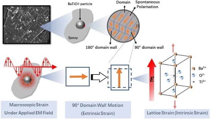
Because of their combination of high strength, high stiffness and low density, advanced polymer composite materials are gaining popularity for applications need high strength, stiffness and low density, such as automobile and aerospace industries. While the main role of these composites has historically been to support certain loads, there is a rising tendency in research to include various secondary functions into composite structures. There is a growing need for materials that combine required functional qualities like load sensing, energy harvesting, temperature monitoring, actuation, etc. with mechanical performance. Moreover, aviation safety standards and assuring structural integrity dependability are critical elements that drive the usage of such materials in aircraft structures. To meet both requirements, non-­destructive inspection of the structure is performed, which is more difficult and expensive than inspecting metallic structures. As a result, new in situ health monitoring approaches must be developed.
In the quest to decrease maintenance costs, remote monitoring of components in systems and structures has become vital. Typically, a health monitoring module with a sensor, wireless telemetry and processing capacity is spread across complicated structures and must function remotely utilising battery power. A battery can only provide power for a certain amount of time before it must be recharged or replaced, resulting in a cost of maintenance. A wireless data transmission module, sensors and an energy harvesting device are often included in a self-­powered health monitoring module. Systems have been extensively researched to convert energy from widely accessible sources such as vibration, human motion, water, air, heat, light and chemical processes into usable electrical energy.
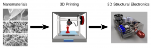
In this chapter, we briefly describe energy harvesting and self-­sensing polymer composites.

Composite powders with carbon nanotubes for laser printing of electronics

Microelectronics Reliability 136, 114718 (2022)

The purpose of this work is to develop electrically conductive composite fine powder containing carbon nanotubes, for use in the laser printing technique. This requires the evaluation of several approaches to the mixing of thermofusible powder with carbon nanotubes. For the experiments, a commercial toner for HP laser printer was used as a matrix and multiwalled carbon nanotubes as a conductive phase. Due to the fine powder morphology, carbon nanotubes should also be compatible with the laser printing technique. Several approaches were evaluated for obtaining a fine composite powder with carbon nanotubes, including ultrasonic stirring and low energy ball milling process. The obtained fine powder was tested towards compatibility with a desktop laser printer. Due to the complexity of the laser printing process, we decided to use the thermal transfer method, one of the elements of the laser printing technique. Adhesive properties evaluations and electrical measurements of powders with various amounts of nanotubes (10–30 wt%) were examined. This allowed selecting the composition of 18–20 wt% of carbon nanotubes as optimal, exhibiting proper adhesion to the paper substrate and with resistance in the range of 102 Ω. For the samples with appropriate adhesion to the substrate, we observe a trend of increasing conductivity with increased nanotube content. The developed composite is compatible with the laser printing technique, but it requires higher pressure than applied by commercial laser printers during the process of melting into the paper substrate.

Electromagnetic field controlled domain wall displacement for induced strain tailoring in BaTiO3-epoxy nanocomposite

Scientific Reports 12, 7504 (2022)


Failure in an epoxy polymer composite material is prone to initiate by the coalescence of microcracks in its polymer matrix. As such, matrix toughening via addition of a second phase as rigid or/and rubber nano/micro-particles is one of the most popular approaches to improve the fracture toughness across multiple scales in a polymer composite, which dissipates fracture energy via deformation mechanisms and microcracks arrest. Few studies have focused on tailorable and variable toughening, so-called ‘active toughening’, mainly suggesting thermally induced strains which offer slow and irreversible toughening due to polymer’s poor thermal conductivity. The research presented in the current article has developed an instantaneous, reversible extrinsic strain field via remote electromagnetic radiation. Quantification of the extrinsic strain evolving in the composite with the microwave energy has been conducted using in-situ real-time fibre optic sensing. A theoretical constitutive equation correlating the exposure energy to micro-strains has been developed, with its solution validating the experimental data and describing their underlying physics. The research has utilised functionalised dielectric ferroelectric nanomaterials, barium titanate (BaTiO3), as a second phase dispersed in an epoxy matrix, able to introduce microscopic electro-strains to their surrounding rigid epoxy subjected to an external electric field (microwaves, herein), as result of their domain walls dipole displacements. Epoxy Araldite LY1564, a diglycidyl ether of bisphenol A associated with the curing agent Aradur 3487 were embedded with the BaTiO3 nanoparticles. The silane coupling agent for the nanoparticles’ surface functionalisation was 3-glycidoxypropyl trimethoxysilane (3-GPS). Hydrogen peroxide (H2O2, 30%) and acetic acid (C2H4O2, 99.9%) used as functionalisation aids, and the ethanol (C2H6O, 99.9%) used for BaTiO3 dispersion. Firstly, the crystal microstructure of the functionalised nanoparticles and the thermal and dielectric properties of the achieved epoxy composite materials have been characterised. It has been observed that the addition of the dielectric nanoparticles has a slight impact on the curing extent of the epoxy. Secondly, the surface-bonded fibre Bragg grating (FBG) sensors have been employed to investigate the real-time variation of strain and temperature in the epoxy composites exposed to microwaves at 2.45 GHz and at different exposure energy. The strains developed due to the in-situ exposure at composite, adhesive and their holding fixture material were evaluated using the FBG. The domain wall induced extrinsic strains were distinguished from the thermally induced strains, and found that the increasing exposure energy has an instantaneously increasing effect on the development of such strains. Post-exposure Raman spectra showed no residual field in the composite indicating no remnant strain field examined under microwave powers < 1000 W, thus suggesting a reversible strain introduction mechanism, i.e. the composite retaining its nominal properties post exposure. The dielectric composite development and quantifications presented in this article proposes a novel active toughening technology for high-performance composite applications in numerous sectors.

Accelerated Testing and Reliability of FDM-Based Structural Electronics

Applied Sciences 12(3), 1110 (2022)

With the development of the miniaturization of electronic systems, heat dissipation from components has become an increasing challenge. Structural electronics represent a new approach to this problem. Instead of downsizing all the elements, in this idea, electronic parts of the device are embedded into its mechanical construction. This approach has many advantages, but the reliability of systems constructed this way has not been extensively studied so far. In this work, circuits consisting of silver ink conductive traces were printed on FDM polymer substrates, with or without 0 Ω resistors, and were subjected to accelerated aging testing. The samples were divided into three groups, and for each of them, the mean time to failure was calculated, which for the best group was 8000 h. This paper also presents the mechanism that led to the failure of these systems, as well as actions that will lead to the elimination of this phenomenon.

Electrically Conductive Nanocomposite Fibers for Flexible and Structural Electronics

Applied Sciences 12(3), 941 (2022)

The following paper presents a simple, low-cost, and repeatable manufacturing process for fabricating conductive, elastic carbon-elastomer nanocomposite fibers for applications in the textile industry and beyond. The presented method allows for the manufacturing of fibers with a diameter of 0.2 mm, containing up to 50 vol. % of graphite powder, 10 vol. % of CNT, and a mix of both fillers. As a result, resistivity below 0.2 Ωm for the 0.2 mm-diameter fibers was achieved. Additionally, conductive fibers are highly elastic, which makes them suitable for use in the textile industry as an element of circuits. The effect of strain on the change in resistance was also tested. Researches have shown that highly conductive fibers can withstand strain of up to 40%, with resistivity increasing nearly five times compared to the unstretched fiber. This research shows that the developed composites can also be used as strain sensors in textronic systems. Finally, functional demonstrators were made by directly sewing the developed fibers into a cotton fabric. First, the non-quantitative tests indicate the feasibility of using the composites as conductive fibers to power components in textronic systems and for bending detection.

Highly conductive electronics circuits from aerosol jet printed silver inks

Scientific Reports 11, 18141 (2021)

Recently, low-cost electronics printed on lightweight, flexible and 3D shaped substrates are gaining importance in the markets of wearables and smart packaging. However, printed electronics do not meet the electrical performance of subtractive techniques because the resistivity of metallic printed patterns is still much higher than that of bulk material. To fulfil this need, low-resistive and easy printable inks for high resolution printed electronics techniques are needed. In this work, parameters of silver nanoparticles ink for micro-scale printed electronics technique, Aerosol Jet Printing, are being enhanced. To increase electrical conductivity and enhance printability, surfactants and dispersing agents were used to increase ultrasonic atomisation efficiency, obtain a uniform structure of printed lines, and narrow the width of printed patterns. Electrical measurements show a decrease in resistivity value in samples enhanced by cationic and non-ionic surfactants, by 95%, compared to initially prepared inks. Surfactant additions to silver nanoparticles Aerosol Jet Printing ink show promising features for application in modern electronics.

Are We Able to Print Components as Strong as Injection Molded?—Comparing the Properties of 3D Printed and Injection Molded Components Made from ABS Thermoplastic

Applied Sciences 2021, 11(15), 6946

In this paper, we are focusing on comparing results obtained for polymer elements manufactured with injection molding and additive manufacturing techniques. The analysis was performed for fused deposition modeling (FDM) and single screw injection molding with regards to the standards used in thermoplastics processing technology. We argue that the cross-section structure of the sample obtained via FDM is the key factor in the fabrication of high-strength components and that the dimensions of the samples have a strong influence on the mechanical properties. Large cross-section samples, 4 × 10 mm2, with three perimeter layers and 50% infill, have lower mechanical strength than injection molded reference samples—less than 60% of the strength. However, if we reduce the cross-section dimensions down to 2 × 4 mm2, the samples will be more durable, reaching up to 110% of the tensile strength observed for the injection molded samples. In the case of large cross-section samples, strength increases with the number of contour layers, leading to an increase of up to 97% of the tensile strength value for 11 perimeter layer samples. The mechanical strength of the printed components can also be improved by using lower values of the thickness of the deposited layers.