Electrical and rheological percolation threshold of graphene pastes for screen-printing

Circuit World, vol. 45, no. 1, pp. 26–30, 2019

A comparison of electric and viscosity percolation threshold is crucial from the scientific and technical points of view to understand the features and capabilities of heterogeneous graphene composite materials and properly select the functional phase volume. Therefore, the purpose of this paper is to present the analysis of the electrical and rheological percolation thresholds in the polymer–graphene screen printing pastes and the analysis of the relation between these two parameters.

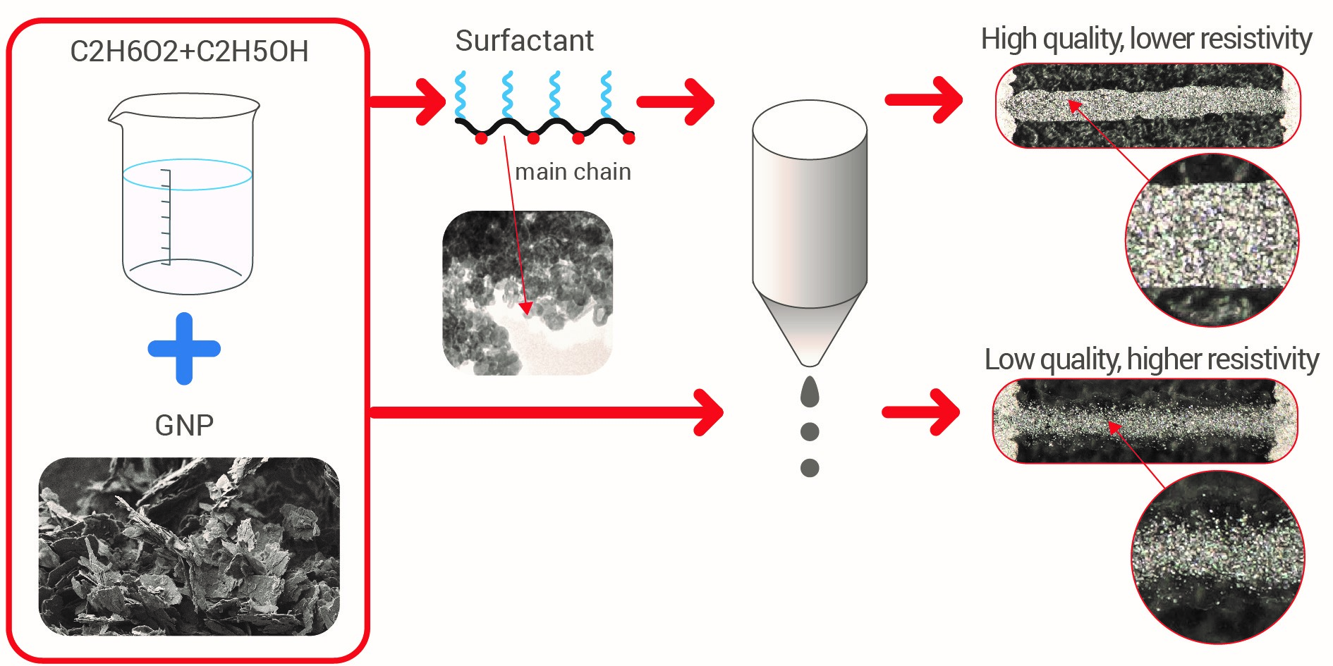
In the paper, the properties of polymer-based pastes with graphene nanoplatelets were tested: paste viscosity and printed layers conductivity. The tests of pastes with different filler content allowed to determine both the electrical and rheological percolation thresholds using power law, according to Kirkpatrick’s percolation model.

The electrical percolation threshold for graphene nanoplatelets (GNPs) in the composite was 0.74 Vol.% when the rheological percolation threshold is observed to be at 1.00 Vol.% of nanoplatelets. The percolation threshold values calculated using the Kirkpatrick’s percolation model were 0.87 and 0.5 Vol.% of GNPs in the paste for electrical and rheological percolation thresholds, respectively.

Recently, GNPs are becoming more popular as the material of the functional phase in screen printing heterophase materials, because of their unique mechanical and electrical properties. However, till date no research presented in the literature is related to the direct comparison of both the electrical and rheological percolation thresholds. Such analysis is important for the optimization of the printing process toward the highest quality of printed conductive paths, and finally the best electrical properties.

Photonic curing of silver paths on 3D printed polymer substrate

Circuit World, Vol. 45 Issue: 1, pp.26-30, 2019

Despite almost limitless possibilities of rapid prototyping, the idea of 3D printed fully functional electronic device still has not been fulfilled – the missing point is a highly conductive material suitable for this technique. The purpose of this paper is to present the usage of the photonic curing process for sintering highly conductive paths printed on the polymer substrate.

This paper evaluates two photonic curing processes for the conductive network formulation during the additive manufacturing process. Along with the xenon flash sintering for aerosol jet-printed paths, this paper examines rapid infrared sintering for thick-film and direct write techniques.

This paper proves that the combination of fused deposition modeling, aerosol jet printing or paste deposition, along with photonic sintering, is suitable to obtain elements with low resistivity of 3,75·10−8 Ωm. Presented outcomes suggest the solution for fabrication of the structural electronics systems for daily-use applications.

The combination of fused deposition modelling (FDM) and aerosol jet printing or paste deposition used with photonic sintering process can fill the missing point for highly conductive materials for structural electronics.

Heterophase materials for fused filament fabrication of structural electronics

Journal of Materials Science: Materials in Electronics, vol. 30, no. 2, pp. 1236–1245, 2018

In this work, new electrically conductive composite filaments are developed for the fabrication of conductive paths, 3D printed with FDM technology. These composite materials consist of electrically conductive copper powder and a polymer matrix. The influence of three different polymers (ABS, PLA, PS) on the electrical properties of the composites was examined. Electrical measurements of the composite filaments with the increasing copper powder concentrations, allow identifying the percolation threshold for elaborated composites. Results show that the lowest resistivity (0.156 × 10−5 Ωm) was achieved for the ABS/Cu composite at the 84.6 wt% Cu concentration. The obtained resistivity values are much lower than for other conductive composites and nanocomposites filaments reported in the literature. Voltage-current characteristics determined for each composite material showed that composites have Ohmic characteristics in low voltage regime. At high voltage regime, the electrical power dissipated in the composites caused a rapid increase in temperature. It was discovered that a polymer matrix influences the maximum value of the electrical power that can be dissipated in the filament before losing electrical conductivity. Examples of conductive 3D printed structures made from elaborated composites are also presented.

Przybył pierwszy w pełni działający smartfon z elastycznym wyświetlaczem.

A zwycięzcą jest …

… Royole ze swoim produktem FlexPai.

Przykro mi Samsungu, LG, Huaweiu, Apple, … 🙁

Efficient Inkjet Printing of Graphene-Based Elements: Influence of Dispersing Agent on Ink Viscosity

Nanomaterials 2018, 8(8), 602

Inkjet printing is an excellent printing technique and an attractive alternative to conventional technologies for the production of flexible, low-cost microelectronic devices. Among many parameters that have a significant impact on the correctness of the printing process, the most important is ink viscosity. During the printing process, the ink is influenced by different strains and forces, which significantly change the printing results. The authors present a model and calculations referring to the shear rate of ink in an inkjet printer nozzle. Supporting experiments were conducted, proving the model assumptions for two different ink formulations: initial ink and with the addition of a dispersing agent. The most important findings are summarized by the process window regime of parameters, which is much broader for the inks with a dispersing agent. Such inks exhibit preferable viscosity, better print-ability, and higher path quality with lower resistivity. Presented results allow stating that proper, stable graphene inks adjusted for inkjet technique rheology must contain modifiers such as dispersing agents to be effectively printed.

Microscale Hybrid Flexible Circuit Printed with Aerosol Jet Technique

IEEE Transactions on Nanotechnology, 2018, V: 17, I:5.

Today, a microprinted electronics circuits are gaining more and more importance, but still printed electronic devices such as transistors or OLEDs are unstable in air and shows a poor performance. Moreover, printed microelectronic elements do not meet quality and high-reliability requirements, essential in electronics applications. To fulfill these needs, hybrid electronic circuits, combining printed technology, and surface-mount technology, are recommended. This approach gets advantages from both methods:Surface-mount devices (SMD) elements provide a high device functionality whereas a printed pattern ensures the device flexibility and efficiency. In this work, silver nanoparticle-based aerosol jet ink (AgNP ink) is used to realize the approach of a hybrid circuit with aerosol jet printed pads and surface-mount devices. The ultrasonic atomization process ensures the high printing resolution and appropriate line formation. Electrical and mechanical characterization was performed to present the connection performance and quality. Cross section view and morphological inspection explain the joint high quality and good performance. Resistance characterization presents the high current conductance comparable with connections made by silver epoxy or ink-jet printing. Shear test results show an excellent connection strength complying with USA Military Standard. Finally, a flexible hybrid conductance touch sensor is manufactured, demonstrating the feasibility of the presented assembling solution.

Pierwsze PRINTduino™ zrobione, a będzie więcej.

Jednym z efektów projektu 3WELES jest przygotowanie demonstratora z obwodem mikrokontrolera, zarówno drukowanego jak i 3D drukowanego, z udziałem elementów dyskretnych. Sam obwód został wykonany z pasty srebrowej na elastycznym podłożu z zastosowaniem techniki sitodruku, a dodatkowe elementy elektroniczne zostały zamontowane z zastosowaniem kleju przewodzącego. To pozwoliło na wykonanie pełnoprawnego klonu Arduino™, ale bazującego na całkowicie wydrukowanych ścieżkach obwodu elektronicznego, zamiast zastosowanie płytki PCB (tylko z nazwy drukowanej). Obecnie pracujemy nad 3D drukowanym PRINTduino™, które zamierzamy wykonać z zastosowaniem opracowanym materiałów i techniki FDM oraz druku bezpośredniego.

Wykonany układ jest efektem pracy dyplomowej „Zastosowanie klejów elektroprzewodzących w montażu obwodów elektroniki drukowanej na podłożach elastycznych i niskotemperaturowych” wykonanej przez Pawła Sawczuka.

Trójwymiarowe elementy elektroniczne wydrukowane techniką druku aerozolowego z zastosowaniem 3D drukowanego robota?

Ufff! Dużo tego “druku”!

Nadchodzi. Zespół dwóch studentów stopnia inżynierskiego i jeden magisterskiego wspólnie budują robota sześcioosiowego wykonanego techniką druku 3D. Rozwiązanie to jest zbiorem kilku projektów dostępnych w internecie, jak: projekt BCN3D, robot autorstwa Andreasa Hoelldorfersa czy ramie robotyczne AR2. Robot będzie częścią nowo zbudowanego stanowiska do wykonywania elementów z zastosowaniem techniki druku aerozolowego.

Będzie problem z dokładnością, funkcjonalność jest niewiadomą, a czy będzie wytrzymały? Tego nie wiemy, ale i tak go zbudujemy, zdobędziemy nowe doświadczenia, a na końcu będzie musiał pracować tak jak my chcemy!

W skład zespołu wchodzą Adrian Wawrzyn, Bartosz Szkoda i Kacper Krętowski, kierowani przez doktoranta Jakuba Krzemińskiego.

Pierwszy demonstrator za nami

Wytężona praca przynosi pierwsze owoce!

Pierwsze eksperymenty nad opracowaniem przewodzącego filamentu dla techniki FFF zaowocowały sukcesem. Potrafimy już wydrukować ścieżki przewodzące w strukturach z polimerowych – a mówiąc „my” mam na myśli doktoranta Bartka Podsiadłego. W kolejce czekają już inne demonstratory, jak drukowana klawiatura, głośnik, cewki i tranzystory, trójwymiarowe Printduino™ (dwuwymiarowe jest łatwe i już zrobione przez nas), … elementy do BFR(?)

Nanomateriały węglowe w technologii elektroniki drukowanej

Książka powstała z potrzeby przedstawienia w prosty i zrozumiały sposób aspektu zastosowania nanomateriałów węglowych w elektronice i zestawienia rozproszonych wyników dorobku zespołów naukowych z całego świata. Konieczność stworzenia takiego opracowania wynika z braku tak obszernie zredagowanej w języku polskim literatury dotyczącej zastosowania nanomateriałów węglowych w elektronice drukowanej, a nawet w literaturze zagranicznej możemy trafić jedynie na bardzo szczegółowe opracowania dotyczące specyficznych rozwiązań, jak zastosowania biomedyczne, optoelektroniczne czy sensorowe. Dodatkowo, czytelnik zainteresowany szerszym spojrzeniem na prace prowadzone w zakresie zastosowania nanomateriałów węglowych w elektronice drukowanej, znajdzie tu wiele odnośników do już opublikowanych opracowań w literaturze krajowej i zagranicznej. W książce przedstawiony jest także dorobek autora związany z opracowaniem drukowanych warstw rezystywnych, elektrod transparentnych, struktur elektroluminescencyjnych, ogniw fotowoltaicznych, czujników wielkości fizycznych i chemicznych, warstw i ścieżek do zastosowań elektroniki wysokich częstotliwości i grzałek. Opisane są szczegółowe badania nad opracowanymi materiałami i strukturami elektronicznymi, obejmujące szereg badań nad właściwościami elektromechanicznymi warstw z nanomateriałami węglowymi, zależności między parametrami procesu nanoszenia a rezystywnością otrzymywanych warstw kompozytowych, oraz charakterystyka mechanizmów przewodnictwa elektrycznego obserwowanych w warstwach kompozytowych z nanomateriałami węglowymi.

Oficyna Wydawnicza Politechniki Warszawskiej, Warszawa, 2017, ISBN 978-83-7814-611-7.

Pełna wersja książki dostępna jest w księgarniach i na platformie wydawniczej IBUK Libra.